Table of Content
However, before even thinking of patching the firmware, making full sense of this dump is needed. Overall, I'm quite happy with how NandBug is working. The NAND Flash dumping and programming features are reliable. This bitstream will generate a FSM that's able to program pages. The pages addresses and data are received from the FT2232H using the Sync FIFO Mode. Everything is now finally ready on the hardware side.

Just start with “Hey Google” to get answers from your Google Assistant, tackle your day, enjoy music or TV shows, and control your compatible smart home devices. And with Voice Match, the Assistant can tell your voice from others—up to six people can get personal assistance on each device. If you want to set up a different device, you can find the instructions in Set up smart devices in the Google Home app.
More by Google LLC
Optionally, a NAND Flash can be directly soldered to the board. A FT2232H. This component adds Hi-Speed USB connectivity to the board. Hardware files are available here while the software can be downloaded from here. I made the schematics, Gerber files, and software of NandBug publicly available. The general idea is in fact to make the NAND Flash of the Google Home in-system programmable. It may sound like an over engineered solution and it maybe is.
This source code will be extremely useful in the second article of this series. In 2014, fail0verflow was able to root Chromecast devices with a vulnerability affecting the bootloader. A buffer overflow vulnerability triggered thanks to a special USB peripheral led to a full secure boot bypass. That said, the Home Mini used a micro-USB port instead of a barrel plug connector, and some people preferred that approach.
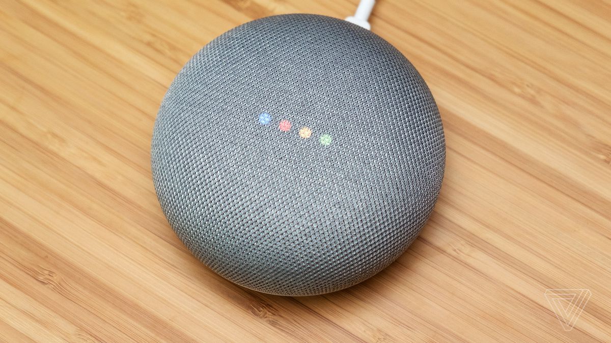
What Is a Google Home Mini and How Does It Work?
” to get answers to the most common privacy and security questions. Its in-store longevity could have been due to Google making too many at launch, and you will undoubtedly find a handful on store shelves if you still really want one. That said, the Home Mini does not appear on Best Buy or Target online stores today.
On the bottom side of the board, only the Interposer Board connector is fitted. Its bitstream format has been reverse-engineered and it is now supported by open source toolchains. A micro-USB connector, used for power and data transfer.
The NandBug System
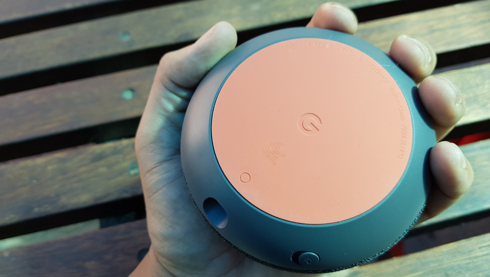
The delicate BGA NAND Flash IC is soldered to this board. As explained before, the SoC of the Google Home Mini comes without any public documentation. Being able to run custom code on it is valuable to understand it better. Things like dumping the BootROM of the system becomes possible.
I guess this nibbles swapping weirdness is caused by the way the low-level hardware BCH engine is actually working. Swap another time the nibbles of the computed BCH code. Swap the nibbles of each of the 2080 first bytes of the page.
Using strings and grep against the firmware dump can quickly reveal interesting bits of information. It was now time to actually have a look at the content of the NAND Flash dump. Playing with the bchlib Python library somewhat confirmed this hypothesis. The length of the ECC data we measured thanks to the graphical visualization could match a BCH-48 algorithm. A glance at the bootloader/berlin_tools/bootloader/nand_ctrl/mv_nand.c file is enough to understand the ECC is calculated by the hardware of the main SoC itself.
Uploading these bitstreams to the FPGA using the SPI Slave Mode programming procedure. Generating one of the four bitstreams detailed above. The bitstream is uploaded to the FPGA by following the protocol described in the iCE40 Programming and Configuration Document. Using these two modes required a special configuration to be burnt to the EEPROM of the FT2232H. The procedure I used to program the correct configuration to the EEPROM is the following.
The first thing to note is that the way the data is written to a NAND Flash is somewhat special. Each page contains data and a special section called OOB, the out-of-bound section. This feature can somehow work a little bit at the very beginning of the Google Home boot sequence though. A this early point, the clock of the NAND Flash peripheral is reduced to a couple of hundred of kHz. More importantly, the Google Home Mini can still boot without problems despite all the heavy surgery it received. Receive the NAND Flash data and compare it to the content of filename.

The Google Home app is designed to show you the status of your home and keep you up to date with what you may have missed. Check in on your home anytime and see a recap of recent events. You can also get a notification if something important happens while you’re away. Turn on the lights, adjust the thermostat, or get an alert when there’s a person or package at your front door. Google Home on WearOS will be available as a preview as we continue to add controls and improvements.
Dynamic analysis of the Goggle Home software running on the actual hardware becomes possible. While extremely informative, the attack described by the presentation cannot be used against my own device anymore. The acoustic hole is on the other side of the PCB. Some RF shields have been removed to expose the components.

As demonstrated in the previous articles of this website, I've always been interested into running my own code on consumer devices. Create Routines that allow you to turn on compatible lights, check the weather, play the news, and more with one simple command. Glad to see that I am not the only one with this problem.
Reading through the init.rc script of the initramfs, it appears these two partitions are YAFFS2 partitions. The Linux Kernel version and compilation timestamp can be extracted from strings present in the binary data. Here, the Linux Kernel command line contains the mtdparts configuration variable. This leaks both the names and sizes of all flash partitions.